
Apple chip builder TSMC not yet ready to move to next-gen lithography system،
The EXE:5000's 8nm resolution means chipmakers can pack more transistors into a single chip. Smaller transistors are more energy efficient, meaning chips will be able to do more with less.-ASML
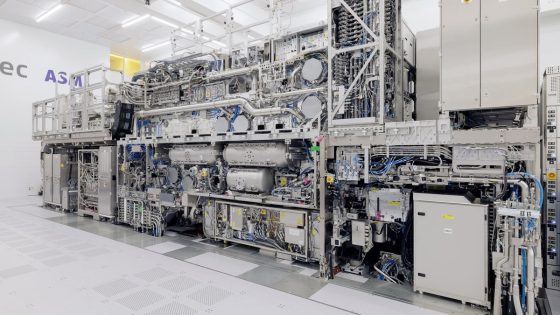
The new EUV High-NA machine features a 0.55 numerical aperture (NA) objective, giving it 8nm resolution compared to current machines' resolution of 13nm (0.33 NA) . This means the new machines can print transistors 1.7 times smaller, resulting in 2.9 times larger transistor densities with a single exposure. The result? More powerful or energy-efficient chips. The new machines can also print 185 wafers per hour, rising to 220 by 2025. This compares to the 160 wafers per hour that can be printed with current EUV machines.
Current EUV Low-NA machines can produce the same resolution, but only after two exposures have been made using a double pattern. However, dual configuration carries risks, including longer production times and an increased risk of a defect occurring. This can also lead to performance variability between manufactured chips.
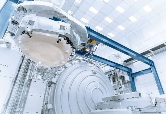
The High-NA EVU mirrors are tested at ZEISS
ASML is quick to tell you what can go wrong with dual modeling, as it would prefer foundries spend the most money on the newest machines. But TSMC's N3B process node, which supposedly relies on a dual configuration, was used to make the A17 Pro application processor used on all of these processors. iPhone 15 Pro And iPhone 15 Pro Max units made by Apple and the M3 chip used to power high-end Macs. ASML says its customers are just now doing their research on EUV High-NA.
Eventually, TSMC, Samsung Foundry and others will need to join Intel and begin making the investments necessary to move to EUV High-NA. That time may soon be here, with TSMC and Samsung looking to start 2nm production in 2025 and move to 1.4nm production in 2027.