Currently, the top two contract foundries are TSMC and Samsung Foundry, with Intel being number three on the rise. According to DigiTimes, instead of expanding its 3nm process node for a few years before moving to 2nm like TSMC is doing, Samsung Foundry is continuing its research and development on 2nm. Recently, Kye Hyun Kyung, head of Samsung’s Semiconductor and Device Solutions (DS) Division, said that in the next five years, Samsung will surpass TSMC and become the world’s leading foundry.
TSMC is estimated to hold 60% of the global foundry market.
Currently, TSMC holds 60% of the global foundry market according to TrendForce.
Samsung, which lost Qualcomm’s business last year due to low yields, is now expected to match TSMC’s 50-60% yield on 3nm production. However, according to semiconductor industry sources, the two companies are focused on different things. TSMC seeks to maintain a stable level of 3nm capacity while Samsung eyes next-generation 2nm production.
Apple is currently the only smartphone manufacturer to offer a phone with a 3nm chipset
In a bid to attract more customers, Samsung Foundry is expected to engage them earlier than usual in the process as production schedules are created, and Samsung hopes this will entice companies to choose its foundry to transform their bullet designs. South Korea money today says the industry expects the 2nm process to gain attention by 2025.
One area where Samsung is ahead of TSMC is in the use of Gate-All-Around (GAA) technology. Using vertically stacked horizontal nanosheets, these transistors can contact the gate on all four sides, reducing current leakage and increasing the drive current. While Samsung Foundry uses GAA with its 3nm process node, TSMC continues to use FinFET transistors for its 3nm production. The current number one foundry will not
start using GAA until it begins mass producing 2nm chips in 2025.
Why all this matters
To put this in simple terms, the reason this is so important is that as the number of process nodes decreases, the size of the transistors decreases. This means that more transistors can be put into a chip, making them more powerful and/or more energy efficient.
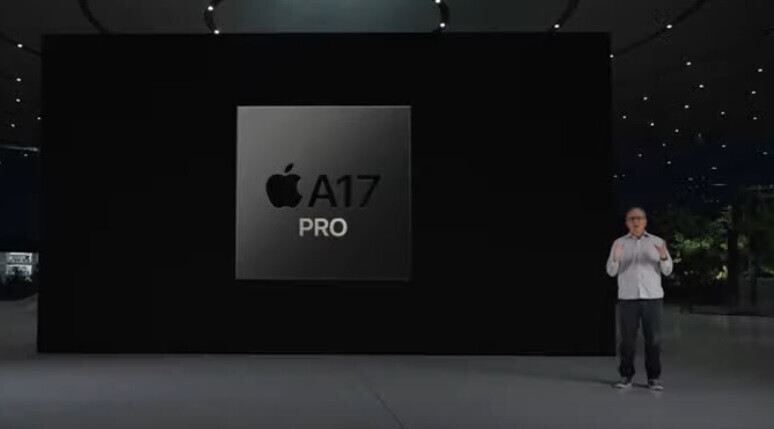
A look at the past few years of Apple’s A-series application processors (APs) illustrates this perfectly:
Although the percentage increase in transistor count varies from year to year and it becomes increasingly difficult to reduce the size of a transistor, you can see that in the example above, Apple has was able to increase the number of transistors inside its A-series chipset by 123%. Put an iPhone 11 Pro Max side by side with a iPhone 15 Pro Max and the difference in speed is immediately felt.
Even though Samsung has a head start at 2nm thanks to early GAA implementation, Apple has been TSMC’s biggest customer for years and we wouldn’t expect to see the Cupertino gang change suppliers of this which is perhaps the most important component used to make an iPhone.
Samsung manufactured Apple’s A-series chips until the A8, produced for the iPhone 6 and iPhone 6 Plus by TSMC in 2014. The A9, designed for the iPhone 6s and iPhone 6s Plus, was built by TSMC and Samsung in 2015. It should be noted that at that time, Apple and Samsung were both embroiled in an ugly patent battle with Apple seeking to reduce its use of Samsung as a supplier. ‘iPhone. For the A10 chip designed for the iPhone 7 range, Apple selected TSMC to manufacture its AP and has remained loyal to the foundry ever since.