Why do we phone enthusiasts go crazy every time a foundry moves to a new process node? The most basic answer I can think of is that as the process node shrinks, so does the size of the transistors used in a chip. Smaller transistors mean that more of them can fit inside a chip, which increases the number of transistors and the higher the number of transistors, the more powerful a chip and/or energy efficient.
A good example that we often use is the
iPhone. In 2019, the iPhone 11 lineup was powered by the 7nm A13 Bionic which contained 8.5 billion transistors. In 2020, the iPhone 12 range was equipped with the 5nm A14 Bionic which carried 11.8 billion transistors. This was followed the following year with the 5nm A15 Bionic used to power the iPhone 13 models. This chip carried 15 billion transistors. The iPhone 14
Pro series featured the 4nm A16 Bionic which contained 16 billion transistors. The iPhone 15 Pro and iPhone 15 Pro Max are currently the only smartphones to use a 3nm chip, the A17 Pro, which has a transistor count of 19 billion.
Currently, even though TSMC and
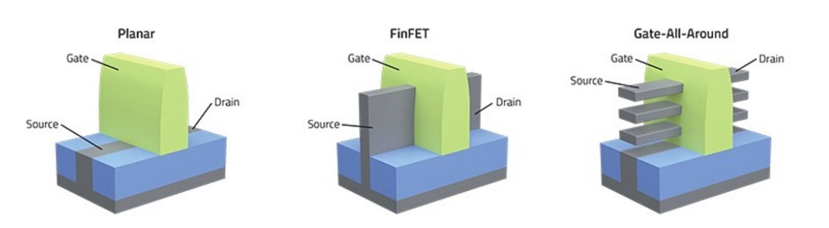
Samsung Foundry can produce chips using their 3nm process nodes, there is a difference between the two companies’ production on this node. While TSMC relies on FinFET transistors, Samsung Foundry uses the next generation Gate-All-Around (GAA) transistors. Using three horizontal nanosheets placed vertically, GAA transistors surround the channel on all four sides of the gate. This reduces current leakage and increases the drive current. TSMC will join Samsung and
start using GAA with its 2nm process node.
By 2025, Intel, Samsung Foundry and TSMC will all use Gate-All-Around transistors
Samsung Foundry will also start mass producing 2nm chips in 2025 and eventually
Tom’s material, in 2027, it is expected to move to the 1.4nm process node. At 1.4nm, Samsung is expected to add a fourth nanosheet that will increase the drive current and improve a chip’s performance by allowing more current to flow through each transistor. Current leakage is further reduced, making chips produced at 1.4nm even more energy efficient. With the increased control of current flow, transistors manufactured at 1.4nm will generate less heat, increasing power efficiency.
As we’ve pointed out, Samsung is getting a head start on TSMC by now using GAA with its 3nm process node. And while TSMC won’t join the club until it hits 2nm in 2025, Intel will beat it in 2024 with its 20A process node that will also use GAA (which it calls RibbonFET). By the time Intel and TSMC start using GAA, Samsung will have experienced it.
All three foundries will also use a 2nm rear power supply (20A for Intel which calls its version Power Via). This moves all power connections from the top of the chip to the bottom, leaving more room for data interconnects above the silicon and helping to create larger power connections at the bottom of the chip. This will also lead to an improvement in the performance of the chip.