China might be licking its lips as Canon reveals tech that could produce 2nm chips without EUV،
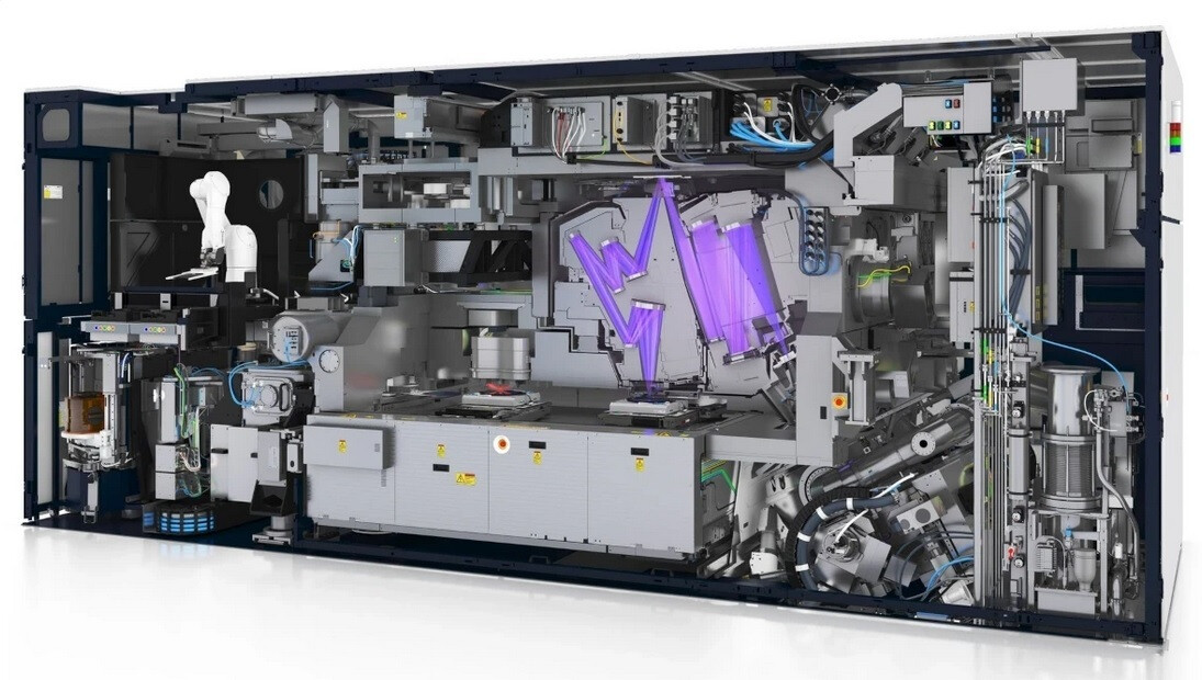
There is only one company in the world that builds $200 million school bus-sized EUV (extreme ultraviolet lithography) machines that are used to etch larger circuit patterns. fine as human hair on a silicon wafer. That company is ASML, a Dutch company that had nearly $26 billion in revenue last year. EUV machines are needed to make chips smaller than 7nm, because you need to etch extremely thin lines to accommodate the billions of transistors built into cutting-edge chips.
Canon announces NIL lithography machine that could challenge EUV technology
Last
week, Canon announced nanoimprint lithography (NIL) technology that it says can be used to produce 5nm chips. EUV machines are used by TSMC and
Samsung Foundry to make 3nm chips with an upgraded machine from ASML soon to be available to handle 2nm production. Both foundries plan to produce 2nm chips as early as 2025. But let’s get back to Canon’s announcement, shall we?
ASML’s extreme ultraviolet lithography machine, which is about the size of a school bus
The Japanese company explains what makes NIL different. “Unlike conventional photolithography equipment, which transfers a circuit pattern by projecting it onto the resin-coated wafer, the new product does this by pressing a printed mask with the circuit pattern onto the resist on the wafer, like a stamp .Because its circuit pattern transfer process does not go through an optical mechanism, the fine circuit patterns on the mask can be faithfully reproduced on the wafer. Thus, complex two- or three-dimensional circuit patterns can be formed in a single print.
Canon says that with improvements in mask technology, NIL will eventually be able to help create 2nm chips. Currently, the technology allows circuit patterns to be etched with a minimum line width of 14nm, which is equivalent to 5nm production. Canon says NIL should support a minimum line width of 10nm, which is equivalent to
building chips using a 2nm process node. NIL can reduce the amount of energy used to make a chip because it does not require a light source with a special wavelength.
Despite the press release, Gartner analyst Gaurav Gupta told The Register: “I would be surprised if Canon suddenly made a major technical breakthrough.” Nanoimprint lithography has been a concept for some time, but problems with defects and other problems have arisen. Memory chip developer SK Hynix and electronics company Toshiba signed a deal in 2015 to develop NIL.
But there is a problem here that the United States will need to resolve quickly. ASML does not ship its EUV machines to China due to US sanctions, but it is possible that since NIL does not use cutting-edge optics or mirrors like EUV does, Canon could ship the technology to China by giving foundries like SMIC (the largest in China), the capacity to produce 5nm and possibly 3nm and 2nm chips.
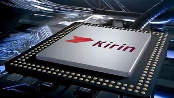
We saw how US lawmakers and officials reacted when Huawei unveiled the Mate 60
Pro powered by a 7nm Kirin 9000s chip with support for 5G. To this day, there are elaborate theories that attempt to explain how SMIC was able to manufacture the chip given the current US export ban. One theory published by tipster The latter was made by TSMC before the ban began in 2020 using its 5nm process node.
Gartner’s Gupta says: “We don’t expect business impact for five years and will
start primarily with memory chips. [being] manufacturing is ready, and that is the challenge. » He expects the United States to soon block the sale of this technology to China.